TEM enables comprehensive characterization crucial for understanding gold nanoparticle assembly. For more on the potential of gold nanoparticles in nanodevices, continue reading.
Image Credit: nararat yong/Shutterstock.com silver plated Cu

Gold nanoparticles are collections of gold particles where the total diameter of the cluster of gold atoms is on the nanometer length scale – typically 1 – 100 nm.1 Gold nanoparticles are normally functionalized, where another chemical species is attached to the surface of the nanoparticle to tune the chemical properties. Often, the chemical groups for functionalization are used to improve properties such as wettability, but for biological applications. They can also be used to improve uptake and biocompatibility.2
Some key applications of gold nanoparticles include photonics, medicine and catalysis.3 Gold nanoparticles have a high absorption cross-section in the visible and infrared regions, which can be tuned by modifying the dimensions of the nanoparticle.
Gold nanoparticles also have strong plasmonic resonance effects, which can be used to enhance the signals for techniques like Raman spectroscopy or to enhance their use in applications such as photothermal therapy, where the particles are used to provide local heating of cells following excitation with light.4
The high degree of tuneability over the size and shape of gold nanoparticles – gold nanoparticles can be spherical clusters but also rods or more complex structures – makes nanoparticles ideal for use as building blocks in nanoscale assemblies. The nanoparticle assembly patterns that can be formed include two-dimensional lattices through self-assembly5 or more complex patterning through direct-write techniques.6
Self-assembling patterns with nanoparticles are very attractive as this can be relatively easy to perform and often requires the evaporation of the local solvent. Although, direct-write or deposition methods offer the opportunity to create more custom methods for making nanoscale devices.
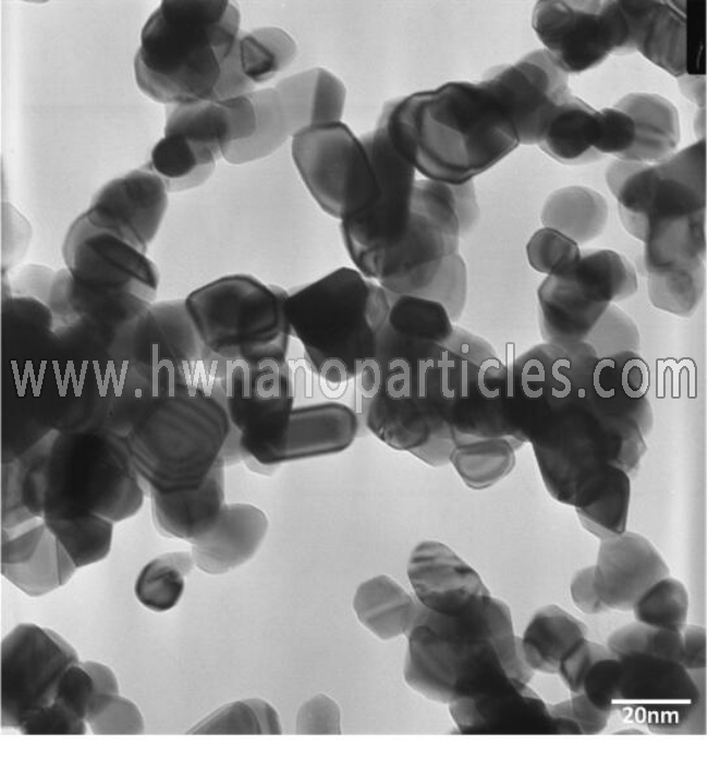
The challenge with creating nanoscale assembly patterns is how to characterize their spatial configuration. The nanoscale nature of nanoparticles means that many standard optical microscopy techniques struggle to resolve individual gold nanoparticles.
Electron microscopes have been invaluable research tools in the nanoscience community due to their extremely high spatial resolutions.7 Transmission electron microscopy (TEM) is routinely used for the study of gold nanoparticles and their characterization, including for the visualization of nanoparticles embedded in pore structures that are just 1-2 nm in size.8
The advantage of TEM for studying gold nanoparticles is that a comprehensive range of information on the nanoparticle composition and structure can be recovered.
Being able to resolve structures below the optical diffraction limit means the nanoparticle can be sized and information on the morphology can be recovered, such as whether the nanoparticle is cubic or rod-like in shape.
It is relatively straightforward to combine energy-dispersive X-ray spectroscopy (EDS) with a TEM instrument that can be used to add further elemental characterization information to the measurement. With sufficiently high spatial resolution TEM, that elemental information can also be used to identify local concentrations of elements from within a nanoparticle.
Image Credit: Georgy Shafeev/Shutterstock.com
Some examples of nanoparticle assembly studies that make use of the capabilities of TEM include the characterization of gold nanocrystal structures.8 Nanocrystals have an assembly pattern that is made up of gold nanoparticle sub-units that form a regular lattice that has a particular shape – much like the atoms do in a normal solid crystalline material.
Nanocrystals are three-dimensional structures, so the TEM images must be recorded in a variety of orientations to look at different crystal planes. This combination of images can then be analyzed to work out the full three-dimensional crystal structure. Beam damage or ionization is a risk with TEM, particularly for smaller dimensional nanocrystals, as it can induce rotation or structural deformation but becomes minimal once the particle size is > 5 nm.8
A large variety of crystalline shapes can be created, but the nanoparticle assembly or growth process is critical in determining the final shape and outcome. For this reason, many researchers have been trying to image the growth process with in situ measurements that make use of methods like TEM to understand and ultimately control the growth mechanisms of nanoassemblies.9
While such imaging measurements can be challenging to carry out, the development of TEM variants such as in situ environmental scanning transmission electron microscopy has meant that the nanoparticle starting solutions can be loaded into the instrument before the growth processes are triggered somehow.
What the researchers could find is that the nanoparticles, when assembled to rods, also seemed to arrange to form colloidally stable 2D assemblies of adjacent nanorods, giving an overall higher dimensionality of structure to the final nanoassembly.
The researchers could also monitor the disassembly process and the role of charge and heat in driving either the assembly or disassembly of the nanoparticle or the introduction of disorder into the overall array.
Typical methods for nanoparticle assembly have relied on self-assembly methods driven by the evaporation of solvent – which requires very careful tuning of the functionalization of the nanoparticles to achieve particular assembly shapes. However, as direct-write methods and the use of electron microscopes to ‘pick up’ and ‘place’ particular atoms become more commonplace, more sophisticated and complex nanoparticle assemblies may emerge for use in nanodevices.
Disclaimer: The views expressed here are those of the author expressed in their private capacity and do not necessarily represent the views of AZoM.com Limited T/A AZoNetwork the owner and operator of this website. This disclaimer forms part of the Terms and conditions of use of this website.
Dr. Rebecca Ingle is a researcher in the field of ultrafast spectroscopy, where she specializes in using X-ray and optical spectroscopies to track precisely what happens during light-triggered chemical reactions.
Please use one of the following formats to cite this article in your essay, paper or report:
Ingle, Rebecca. (2024, February 05). Characterizing Gold Nanoparticle Assembly Patterns Through TEM. AZoNano. Retrieved on February 05, 2024 from https://www.azonano.com/article.aspx?ArticleID=6685.
Ingle, Rebecca. "Characterizing Gold Nanoparticle Assembly Patterns Through TEM". AZoNano. 05 February 2024. <https://www.azonano.com/article.aspx?ArticleID=6685>.
Ingle, Rebecca. "Characterizing Gold Nanoparticle Assembly Patterns Through TEM". AZoNano. https://www.azonano.com/article.aspx?ArticleID=6685. (accessed February 05, 2024).
Ingle, Rebecca. 2024. Characterizing Gold Nanoparticle Assembly Patterns Through TEM. AZoNano, viewed 05 February 2024, https://www.azonano.com/article.aspx?ArticleID=6685.
Do you have a review, update or anything you would like to add to this article?
David Morris of ICSPI highlights the Redux AFM's ease of use, enhancing AFM accessibility for nanoscale imaging.
We speak with Professor Hongxia Wang from QUT about a new project that hopes to utilize graphene and other low-cost carbon materials to produce commercially viable, ultra low-cost, flexible perovskite solar cells.
Moti Segev & Vlad Shalaev
In this interview, AzoNano speaks to Professor Moti Segev and Professor Vladimir Shalaev, who made surprising discoveries about photonic time crystals that challenge existing research and theories.
The NanoWizard ULTRA Speed 3 BioAFM by Bruker combines advanced optical microscopy and super-resolution techniques to provide correlated sample measurements and in-depth nanomechanical characterization.
The Asylum Research Jupiter XR Atomic Force Microscope from Oxford Instruments is the first and only large-sample AFM to offer both high-speed imaging and extended range in a single scanner.
This product profile describes the features and applications of the alpha300 Semiconductor Edition Raman microscope for chemical imaging.
AZoNano.com - An AZoNetwork Site
Iridium Nanoparticles Owned and operated by AZoNetwork, © 2000-2024